CPU variants: Difference between revisions
(UA6527P clock divider) |
(Added some info and added links to the forum posts i used in this (and the previous edit) to the bottom. There are lots more CPU / PPU clones in those threads, but i don't have the time to add them right now.) |
||
| (32 intermediate revisions by 7 users not shown) | |||
| Line 1: | Line 1: | ||
Beyond the well-studied 2A03G, we know of the following CPU revisions, both made by Ricoh and other manufacturers: | Beyond the well-studied 2A03G, we know of the following CPU revisions, both made by Ricoh and other manufacturers: | ||
{| class="tabular" | ==Official (NTSC)== | ||
{| class="tabular sortable" | |||
! class="unsortable"| Part | |||
! class="unsortable"| Picture | |||
! class="unsortable"| Notes | |||
|- | |- | ||
| | | RP2A03 | ||
[[File:CPU= | | [[File:RP2A03_3G1_09.jpg|400px]] [[File:CPU=RP2A03 3L4 27.jpg|400px]] [[File:CPU=RP2A03 3M294.jpg|400px]] | ||
| M2 duty cycle is 17/24 instead of 15/24 [https://forums.nesdev.org/viewtopic.php?p=166761#p166761]. Lacks tonal noise mode. [[APU Frame Counter]] not restarted on reset. Has broken and disabled [[RP2A03 Programmable Interval Timer|programmable interval timer]] on-die. Pin 30 connects to nothing. Other differences? | |||
|- | |- | ||
| | | RP2A03E | ||
[[File:CPU= | | [[File:CPU=RP2A03E 5K5 26.jpg|400px]] [[File:CPU=RP2A03E VF4109 5H4 8534.jpg|400px]] | ||
| Pin 30 is /RDY - combined with internal signals before feeding to internal 6502 +RDY. | |||
|- | |- | ||
| | | RP2A03G | ||
[[File:CPU= | | [[File:CPU=RP2A03G 9B3 PV A.jpg|400px]] [[File:CPU=RP2A03G 8815AAL.jpg|400px]] | ||
| Reference model. Pin 30 enables a [[CPU Test Mode|CPU test mode]]. Later runs introduced a DMC DMA bug [https://forums.nesdev.org/viewtopic.php?p=275359#p275359]. | |||
|- | |- | ||
| | | RP2A03H | ||
[[File:CPU= | | [[File:CPU=RP2A03H 4AM 4F.jpg|400px]] [[File:CPU=RP2A03H 4BM 4Z.jpg|400px]] | ||
| No known differences from late RP2A03G. | |||
|- | |- | ||
| | | RP2A04 | ||
[[File:CPU= | | [[File:CPU=RP2A04 2J 6C2 01.jpg|400px]] | ||
| Not actually a CPU at all, just a jumper in a 40-pin PDIP. Used in place of CPUs in [[Vs. System]] boards (and thus with NTSC timing). | |||
|} | |||
==Official (PAL)== | |||
{| class="tabular" | |||
! class="unsortable"| Part | |||
! class="unsortable"| Picture | |||
! class="unsortable"| Notes | |||
|- | |- | ||
| | | RP2A07 | ||
[[File:CPU= | | [[File:CPU=RP2A07 7C4 39.jpg|400px]] [[File:CPU=RP2A07 8F3 78.jpg|400px]] | ||
| Input clock divider is 16. M2 duty cycle is 19/32 [https://forums.nesdev.org/viewtopic.php?p=166761#p166761]. Changes to noise, DPCM, frame timer tables. Fixed DPCM RDY address bus glitches. Pin 30 connects to 6502 /RDY input. | |||
|- | |- | ||
| MG-N-501 | | RP2A07A | ||
| [[File:CPU=RP2A07A 1GM 36.jpg|400px]] [[File:CPU=RP2A07A 2JM 3L.jpg|400px]] | |||
| no known differences relative to 2A07letterless | |||
|} | |||
==Unofficial== | |||
{| class="tabular" | |||
! class="unsortable"| Part | |||
! class="unsortable"| Picture | |||
! class="unsortable"| Notes | |||
|- | |||
| MG-N-501 | |||
| [[File:CPU=MG-N-501 8933.jpg|400px]] | |||
| | |||
|- | |- | ||
| [https://forums.nesdev.org/viewtopic.php?p=154574#p154574 MG-P-501] || Micro Genius-made clone. Die has the same (UMC) © Ⓜ B6167F marking as a UA6527P. | | [https://forums.nesdev.org/viewtopic.php?p=154574#p154574 MG-P-501] | ||
| [[File:CPU=MG-P-501 9221S 415521.jpg|400px]] | |||
| Micro Genius-made clone. Die has the same (UMC) © Ⓜ B6167F marking as a UA6527P. | |||
|- | |- | ||
| UA6527 | | | UA6527 | ||
[[File:CPU=UA6527-8909-BS.jpg|400px]] [[File:CPU=UA6527-9310-CG-C12520.jpg|400px]] | | [[File:CPU=UA6527-8909-BS.jpg|400px]] [[File:CPU=UA6527-9310-CG-C12520.jpg|400px]] | ||
| UMC-made clone of 2A03G. Has swapped pulse channel duty cycles. Input clock Divider is 12. | |||
|- | |- | ||
| UA6527P || UMC-made clone of 2A03G for compatibility with NTSC software in PAL countries. input clock divider | | rowspan=4|UA6527P || colspan=2|UMC-made clone of 2A03G for compatibility with NTSC software in PAL countries. Different input clock divider. Still has swapped pulse channel duty cycles. Otherwise believed same as 6527. | ||
One revision has (UMC) © Ⓜ B6167F 1989 09 on the die. | One revision has (UMC) © Ⓜ B6167F 1989 09 on the die. | ||
DMC status bit is cleared 1 APU cycle later than on RP2A03 CPUs. The cause is not known. This changes the timing for [[DMA#Bugs|DMC DMA implicit-stop glitches]] (the sample must be started 1 APU cycle earlier to trigger the glitches), and it is suspected that it delays DMC IRQ by 1 APU cycle. Noise channel is slightly louder than others. | |||
| [[File:CPU=UA6527P 8931S.jpg|400px]] || Runs hot. Revisions without "-" in the date stamp have a ÷16 CPU divider | |- | ||
| [[File:CPU=UA6527P 8931S.jpg|400px]] || Runs hot. Revisions without "-" in the date stamp have a ÷16 CPU divider, like 6540 and 2A07 | |||
|- | |- | ||
| [[File:CPU=UA6527P 9019-BS.jpg|400px]] || Runs hot. Revisions with "-" in the date stamp have a ÷15 CPU divider | | [[File:CPU=UA6527P 9019-BS.jpg|400px]] || Runs hot. Revisions with "-" in the date stamp have a ÷15 CPU divider | ||
|- | |- | ||
| [[File:CPU=UA6527P 9214-BS 310551.jpg|400px]] || Runs cooler | | [[File:CPU=UA6527P 9214-BS 310551.jpg|400px]] || Runs cooler | ||
|- | |- | ||
| UA6540 || UMC-made clone of 2A07 [https://forums.nesdev.org/viewtopic.php?t=17257]. Has swapped pulse duty cycles. | | UA6527PQ | ||
[ | | [[File:CPU=UA6527PQ 9306.JPG|400px]] | ||
| | |||
|- | |||
| UA6540 | |||
| [[File:CPU=UA6540 8833S.JPG|400px]] [[File:CPU=UA6540-8834S.jpg|400px]] | |||
| UMC-made clone of 2A07 [https://forums.nesdev.org/viewtopic.php?t=17257]. Has swapped pulse duty cycles. | |||
Subsequent research implies this is identical to the early 6527P - NTSC tuning tables, ÷16 CPU divider. [https://forums.nesdev.org/viewtopic.php?p=283514#p283514] | |||
|- | |||
| UM6547 | |||
| [[File:CPU=UA6547 8950S.JPG|400px]] | |||
| Believed to be a 100% duplicate of UA6527, for use in PAL-M region. | |||
|- | |- | ||
| UM6557 || Believed to be a 100% duplicate of UA6527, for use in SECAM regions. | | UM6557 | ||
| [[File:UM6557.JPG|400px]] | |||
| Believed to be a 100% duplicate of UA6527, for use in SECAM regions. | |||
|- | |- | ||
| UM6561xx-1 || NES-on-a-chip for NTSC. Revisions "xx" AF, BF, CF | | UM6561xx-1 | ||
| No Picture | |||
| NES-on-a-chip for NTSC. Revisions "xx" F, AF, BF, CF known. | |||
|- | |- | ||
| UM6561xx-2 || NES-on-a-chip for PAL-B. Revisions "xx" AF, BF, CF | | UM6561xx-2 | ||
| [[File:NOAC=UM6561_AF-2 9440A R81040.jpg|200px]] [[File:UM6561F-2.jpg]] | |||
| NES-on-a-chip for PAL-B. Revisions "xx" F, AF, BF, CF known. | |||
F and AF revision pulse wave duty cycles match RP2A03, and DMC status bit is cleared 1 APU cycle later than on RP2A03 CPUs. | |||
AF revision observed to have incorrect ASR #imm ($4B) behavior, but other stable illegal instructions work properly. | |||
|- | |- | ||
| | | 1818N | ||
| [[File:CPU = 1818N 9218.png|200px]] | |||
| ??-made NES-on-a-chip, NTSC timing. | |||
|- | |||
| T1818P | |||
| [[File:1818P 0.jpeg|200px]] | |||
| ??-made NES-on-a-chip[[//forums.nesdev.org/viewtopic.php?p=228515#p228515]. Requires external 2 KiB RAMs for CPU and PPU. Swapped pulse duty cycles. DMC status bit is cleared 1 APU cycle later than on RP2A03 CPUs. | |||
|- | |||
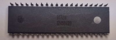
| TA-03N | |||
| [[File:CPU=TA-03N 6527 9250.jpg|400px]] | |||
[[File:CPU=TA-03N 9172N 12450820.jpg|400px]] | |||
| ??-made die-mask clone of 2A03G. Chip underside also has two codes of currently unknown purpose. Pin 30 activates CPU Test Mode like on 2A03G. Clock Divisor is 12. Illegal opcodes are the same. Early 1991 dated chips are reported to have problems with APU DMC playback, but this was corrected in 1992 onward. Runs hot. | |||
|- | |||
| TA-03NP | |||
| [[File:CPU=TA-03NP EWP0124.jpg|400px]] | |||
| ??-made clone of 2A03G for NTSC compatibility in PAL countries. Input clock divider is 15? | |||
But not this one, this input clock divider is 12. | |||
|- | |||
| TA-03NP1 | |||
| [[File:CPU=TA-03NP1 6527P 9231.jpg|400px]] | |||
| ??-made clone of 2A03G for NTSC compatibility in PAL countries. Input clock divider is 15. Fixed DPCM problems? Correct pulse channel duties. Noise channel is slightly louder than others. DMC status bit is cleared 1 APU cycle later than on RP2A03 CPUs. | |||
|- | |- | ||
| | | PM03 | ||
| [[File:CPU=PM03 HI25.jpg|400px]] | |||
| [[wikipedia:IGB_Eletr%C3%B4nica|Gradiente]]-made clone of 2A03G. [https://forums.nesdev.org/viewtopic.php?p=195175#p195175] | |||
|- | |- | ||
| | | GS870007 | ||
| [[File:CPU=GS87007 8827.jpg|400px]] | |||
| (Goldstar??)-made clone of 2A03 - has functioning decimal mode? [http://gxemu.blog67.fc2.com/blog-entry-363.html] <!-- https://archive.ph/70J8j --> | |||
|- | |- | ||
| | | KC-6005 | ||
| [[File:CPU=KC-6005.jpg|400px]] | |||
[[File:CPU= | | Found in MT777-DX famiclone, behaves exactly like UA6527P | ||
|- | |||
| 6005B | |||
| [[File:CPU=6005B.jpg|400px]] | |||
| | |||
|- | |||
| 2011 | |||
| [[File:CPU=2011.jpg|400px]] | |||
| | |||
|- | |||
| “2A03E” | |||
| [[File:CPU=USC 2A03E 9118S 314531.jpg|400px]] [[File:CPU=2A03E 9122A 422951.jpg|100px]] | |||
| Both with and without USC insignia | |||
|- | |||
| KP2B03E | |||
| [[File:CPU=KP2B03E DHG 44.jpg]] | |||
| | |||
|- | |||
| 6527-21 | |||
| [[File:CPU=6527-21 P03 9211M 7056.png|400px]] | |||
| | |||
|- | |||
| 6527P | |||
| [[File:CPU=6527P CFE1 1PC.png|400px]] [[File:CPU=6527P CKD1 1PC.png|400px]] | |||
| | |||
|- | |||
| HA6527P | |||
| [[File:CPU=HA6527P CAKBS.png|400px]] [[File:CPU=HA6527P CX66.png|400px]] | |||
| | |||
|- | |- | ||
| | | 6527P-SS-P03 | ||
[[File:CPU= | | [[File:CPU=SENITON 6527P-SS-P03.png|400px]] | ||
| | |||
|- | |- | ||
| | | 6527UP-8 | ||
[[File:CPU= | | [[File:CPU=SENiTON 6527UP-8.png|400px]] | ||
| | |||
|- | |- | ||
| | | 6527AP | ||
[[File:CPU= | | [[File:CPU=SENiTON 9118C 6527AP.png|400px]] [[File:CPU=SENiTON 9122C 6527AP CFDC.png|400px]] | ||
| | |||
|- | |- | ||
| | | SL/WH6527AP | ||
[[File:CPU= | | [[File:CPU=SL-WH6527AP 9117.png|400px]] | ||
| | |||
|- | |- | ||
| | | SNC6527P | ||
| [[File:CPU=SNC6527P 9116.png|400px]] | |||
| | |||
|- | |- | ||
| | | XYZ-6783 | ||
| [[File:CPU = XYZ-6783 9129.jpg|400px]] | |||
| Lacks tonal noise mode like original RP2A03, but resets APU Frame Counter on console reset like 2A03E/2A03G. Otherwise behaves like letterless RP2A03. | |||
|- | |- | ||
| | | 6538N | ||
[[File:CPU= | | [[File:CPU = 6538N CW6B 3NQ.jpg|400px]] | ||
| ??-made CPU, despite the part number being similar to UMC PPU. Has inverted duty cycles like UA6527. DPCM works. | |||
|- | |- | ||
| | | 8Z01N | ||
| [[File:8Z01N CPU.jpg|400px]] | |||
| | |||
|} | |} | ||
| Line 93: | Line 204: | ||
== See also == | == See also == | ||
* [[PPU variants]] | |||
* https://forums.nesdev.org/viewtopic.php?p=45889#p45889 | * https://forums.nesdev.org/viewtopic.php?p=45889#p45889 | ||
* https://forums.nesdev.org/viewtopic.php?t=23916 (More Info on CPU Clones) | |||
* https://forums.nesdev.org/viewtopic.php?t=23682 (Lots of Images and die-shots) | |||
Latest revision as of 16:41, 11 October 2024
Beyond the well-studied 2A03G, we know of the following CPU revisions, both made by Ricoh and other manufacturers:
Official (NTSC)
| Part | Picture | Notes |
|---|---|---|
| RP2A03 |   
|
M2 duty cycle is 17/24 instead of 15/24 [1]. Lacks tonal noise mode. APU Frame Counter not restarted on reset. Has broken and disabled programmable interval timer on-die. Pin 30 connects to nothing. Other differences? |
| RP2A03E |  
|
Pin 30 is /RDY - combined with internal signals before feeding to internal 6502 +RDY. |
| RP2A03G |  
|
Reference model. Pin 30 enables a CPU test mode. Later runs introduced a DMC DMA bug [2]. |
| RP2A03H |  
|
No known differences from late RP2A03G. |
| RP2A04 | 
|
Not actually a CPU at all, just a jumper in a 40-pin PDIP. Used in place of CPUs in Vs. System boards (and thus with NTSC timing). |
Official (PAL)
| Part | Picture | Notes |
|---|---|---|
| RP2A07 |  
|
Input clock divider is 16. M2 duty cycle is 19/32 [3]. Changes to noise, DPCM, frame timer tables. Fixed DPCM RDY address bus glitches. Pin 30 connects to 6502 /RDY input. |
| RP2A07A |  
|
no known differences relative to 2A07letterless |
Unofficial
| Part | Picture | Notes |
|---|---|---|
| MG-N-501 | 
|
|
| MG-P-501 | 
|
Micro Genius-made clone. Die has the same (UMC) © Ⓜ B6167F marking as a UA6527P. |
| UA6527 |  
|
UMC-made clone of 2A03G. Has swapped pulse channel duty cycles. Input clock Divider is 12. |
| UA6527P | UMC-made clone of 2A03G for compatibility with NTSC software in PAL countries. Different input clock divider. Still has swapped pulse channel duty cycles. Otherwise believed same as 6527.
One revision has (UMC) © Ⓜ B6167F 1989 09 on the die. DMC status bit is cleared 1 APU cycle later than on RP2A03 CPUs. The cause is not known. This changes the timing for DMC DMA implicit-stop glitches (the sample must be started 1 APU cycle earlier to trigger the glitches), and it is suspected that it delays DMC IRQ by 1 APU cycle. Noise channel is slightly louder than others. | |
 |
Runs hot. Revisions without "-" in the date stamp have a ÷16 CPU divider, like 6540 and 2A07 | |
 |
Runs hot. Revisions with "-" in the date stamp have a ÷15 CPU divider | |
 |
Runs cooler | |
| UA6527PQ | 
|
|
| UA6540 |  
|
UMC-made clone of 2A07 [4]. Has swapped pulse duty cycles.
Subsequent research implies this is identical to the early 6527P - NTSC tuning tables, ÷16 CPU divider. [5] |
| UM6547 | 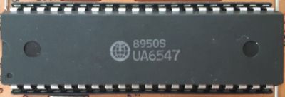
|
Believed to be a 100% duplicate of UA6527, for use in PAL-M region. |
| UM6557 | 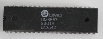
|
Believed to be a 100% duplicate of UA6527, for use in SECAM regions. |
| UM6561xx-1 | No Picture | NES-on-a-chip for NTSC. Revisions "xx" F, AF, BF, CF known. |
| UM6561xx-2 | 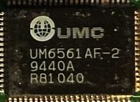 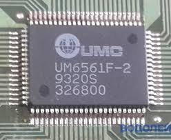
|
NES-on-a-chip for PAL-B. Revisions "xx" F, AF, BF, CF known.
F and AF revision pulse wave duty cycles match RP2A03, and DMC status bit is cleared 1 APU cycle later than on RP2A03 CPUs. AF revision observed to have incorrect ASR #imm ($4B) behavior, but other stable illegal instructions work properly. |
| 1818N | 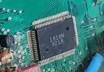
|
??-made NES-on-a-chip, NTSC timing. |
| T1818P | 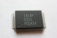
|
??-made NES-on-a-chip[[6]. Requires external 2 KiB RAMs for CPU and PPU. Swapped pulse duty cycles. DMC status bit is cleared 1 APU cycle later than on RP2A03 CPUs. |
| TA-03N | 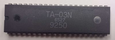
|
??-made die-mask clone of 2A03G. Chip underside also has two codes of currently unknown purpose. Pin 30 activates CPU Test Mode like on 2A03G. Clock Divisor is 12. Illegal opcodes are the same. Early 1991 dated chips are reported to have problems with APU DMC playback, but this was corrected in 1992 onward. Runs hot. |
| TA-03NP | 
|
??-made clone of 2A03G for NTSC compatibility in PAL countries. Input clock divider is 15?
But not this one, this input clock divider is 12. |
| TA-03NP1 | 
|
??-made clone of 2A03G for NTSC compatibility in PAL countries. Input clock divider is 15. Fixed DPCM problems? Correct pulse channel duties. Noise channel is slightly louder than others. DMC status bit is cleared 1 APU cycle later than on RP2A03 CPUs. |
| PM03 | 
|
Gradiente-made clone of 2A03G. [7] |
| GS870007 | 
|
(Goldstar??)-made clone of 2A03 - has functioning decimal mode? [8] |
| KC-6005 | 
|
Found in MT777-DX famiclone, behaves exactly like UA6527P |
| 6005B | 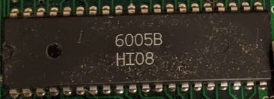
|
|
| 2011 | 
|
|
| “2A03E” |  
|
Both with and without USC insignia |
| KP2B03E | 
|
|
| 6527-21 | 
|
|
| 6527P | 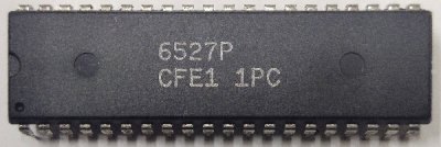 
|
|
| HA6527P |  
|
|
| 6527P-SS-P03 | 
|
|
| 6527UP-8 | 
|
|
| 6527AP |  
|
|
| SL/WH6527AP | 
|
|
| SNC6527P | 
|
|
| XYZ-6783 | 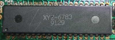
|
Lacks tonal noise mode like original RP2A03, but resets APU Frame Counter on console reset like 2A03E/2A03G. Otherwise behaves like letterless RP2A03. |
| 6538N | 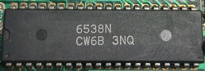
|
??-made CPU, despite the part number being similar to UMC PPU. Has inverted duty cycles like UA6527. DPCM works. |
| 8Z01N | 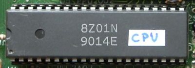
|
|
If you know of other differences or other revisions, please add them!
See also
- PPU variants
- https://forums.nesdev.org/viewtopic.php?p=45889#p45889
- https://forums.nesdev.org/viewtopic.php?t=23916 (More Info on CPU Clones)
- https://forums.nesdev.org/viewtopic.php?t=23682 (Lots of Images and die-shots)
