CPU variants: Difference between revisions
From NESdev Wiki
Jump to navigationJump to search
(Adds links. Improves pin 30 and DMC DMA notes.) |
(mention 2A03 difference even though it's also on CPU power up state) |
||
| Line 2: | Line 2: | ||
{| class="tabular" | {| class="tabular" | ||
| RP2A03 || M2 duty cycle is 17/24 instead of 15/24 [https://forums.nesdev.org/viewtopic.php?p=166761#p166761]. Lacks tonal noise mode. Has broken and disabled [[RP2A03 Programmable Interval Timer|programmable interval timer]] on-die. Pin 30 connects to nothing. Other differences? | | RP2A03 || M2 duty cycle is 17/24 instead of 15/24 [https://forums.nesdev.org/viewtopic.php?p=166761#p166761]. Lacks tonal noise mode. [[APU Frame Counter]] not restarted on reset. Has broken and disabled [[RP2A03 Programmable Interval Timer|programmable interval timer]] on-die. Pin 30 connects to nothing. Other differences? | ||
|- | |- | ||
| RP2A03E || Pin 30 may connect to 6502 /RDY input. | | RP2A03E || Pin 30 may connect to 6502 /RDY input. | ||
Revision as of 02:10, 13 September 2022
Beyond the well-studied 2A03G, we know of the following CPU revisions, both made by Ricoh and other manufacturers:
| RP2A03 | M2 duty cycle is 17/24 instead of 15/24 [1]. Lacks tonal noise mode. APU Frame Counter not restarted on reset. Has broken and disabled programmable interval timer on-die. Pin 30 connects to nothing. Other differences? |
| RP2A03E | Pin 30 may connect to 6502 /RDY input. |
| RP2A03G | Reference model. Pin 30 enables a CPU test mode. Later runs may have introduced a DMC DMA bug [2]. |
| RP2A03H | No known differences from late RP2A03G. |
| RP2A04 | Not actually a CPU at all, just a jumper in a 40-pin PDIP |
| RP2A07 | input clock divider is 16. M2 duty cycle is 19/32 [3]. Changes to noise, DPCM, frame timer tables. Fixed DPCM RDY address bus glitches. Pin 30 connects to 6502 /RDY input. |
| RP2A07A | no known differences relative to 2A07letterless |
| MG-P-501 | Micro Genius-made clone. Die has the same (UMC) © Ⓜ B6167F marking as a UA6527P. |
| UA6527 | UMC-made clone of 2A03G. Has swapped pulse channel duty cycles. |
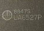
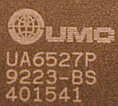
| UA6527P | UMC-made clone of 2A03G for compatibility with NTSC software in PAL countries. input clock divider is 15. Otherwise believed same as 6527.
Two revisions exist: before mid-1990 (which has UMC logo on left) and after-mid-1990 (which has UMC logo on top). It is said that old UMC CPU has broken DMC reader function [4]. Addidionally it has input clock divider equals to 16 in contrary to the 15 present in newer one, that would explain why some games work differently (for example: CodeMasters' titles) One revision has (UMC) © Ⓜ B6167F 1989 09 on the die. |
| UA6540 | UMC-made clone of 2A07 [5]. Has swapped pulse duty cycles. |
| UM6557 | Believed to be a 100% duplicate of UA6527, for use in SECAM regions. |
| UM6561xx-1 | NES-on-a-chip for NTSC. Revisions "xx" AF, BF, CF, F known. Earlier revisions (which?) CPU half believed identical to UA6527; later revisions correct pulse channel duties. |
| UM6561xx-2 | NES-on-a-chip for PAL-B. Revisions "xx" AF, BF, CF, F known. Earlier revisions (which?) CPU half believed identical to UA6527P; later revisions correct pulse channel duties.
"AF" revision pulse wave duties observed to be same as 2A03. |
| T1818 | ??-made NES-on-a-chip, NTSC timing. Believed to exist, but evidence currently scant. |
| T1818P | ??-made NES-on-a-chip[[6]. Requires external 2 KiB RAMs for CPU and PPU. Swapped pulse duty cycles. |
| TA-03N | ??-made clone of 2A03G. Pin 30 selects input clock divider? |
| TA-03NP | ??-made clone of 2A03G for NTSC compatibility in PAL countries. Input clock divider is 15. |
| TA-03NP1 | ??-made clone of 2A03G for NTSC compatibility in PAL countries. Input clock divider is 15. Fixed DPCM problems? |
| PM03 | Gradiente-made clone of 2A03G. [7] |
| GS870007 | (Goldstar??)-made clone of 2A03 - has functioning decimal mode? [8] |
| KC-6005 | Found in MT777-DX famiclone, behaves exactly like UA6527P |
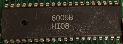
| 6005B | 
|
| 2011 | 
|
If you know of other differences or other revisions, please add them!


