Visual circuit tutorial
This is a crash course on making sense of the circuit displays in Visual 6502/2C02/2A03, written for people without much low-level electronics experience (like the author). It aims to present the information needed to read the diagrams at a basic level in simple language, omitting details that are unimportant when starting out.
You might want to read the Visual 6502 user's guide and the Visual 2C02 page first.
What the different colored areas are
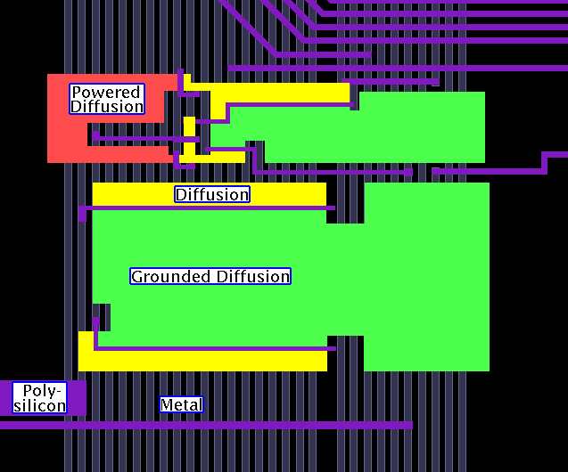
Let's start by defining what the different colors mean:
- Green areas are diffusion (explained below) connected to ground.
- Red areas are diffusion connected to VCC (power).
- Yellow areas are diffusion that is neither connected directly to ground nor directly to VCC.
- Gray areas are metal.
- Purple areas are polysilicon (often shortened to just "poly").
At the level presented here, diffusion, metal, and polysilicon can be thought of as roughly equivalent when viewed in isolation; they all conduct current. The important difference is in how they interact with each other, which is explained below.
Basic building blocks
Transistors
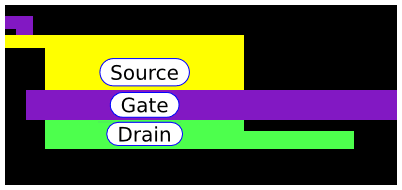
When a piece of polysilicon is sandwiched between two areas of diffusion, it acts as a gate, only letting current through when the polysilicon is powered (or, equivalently, high, 1, or open). The diffusion area from which current will flow when the gate is open is called the source. The diffusion area into which current will flow is called the drain. The gate together with the source and drain is what makes a transistor.
Power sources
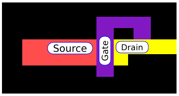
Around an area of powered diffusion we will often see something like the following (note the distinctive "hook" in the polysilicon):
Here the polysilicon acts roughly like a resistor, preventing a short from VCC to ground when the power source would otherwise have a direct connection to ground along some path of open gates.
Nodes
Electrically common areas are called nodes in Visual 6502/2C02/2A03. Clicking on a node will highlight it, making it easier to see how things are connected (clicking on powered or grounded diffusion won't work; these only modify properties of other nodes and are not themselves nodes). When a node is highlighted, a numeric ID unique to the node will be displayed in the upper right, along with a name for the node if it has one. Node names are defined in nodenames.js.
The Find: edit field can be used to locate nodes, either by numeric ID or by name. Numeric IDs can also be used to trace the values of nodes without an assigned name.
Logic elements
Inverters
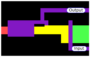
An inverter is constructed like in the image below:
When the input gate is low, current flows into the output wire. When the input gate is high, current flows into ground, driving the output wire low. The output wire is hence the inverse of the input wire.
When one node is the inverse of another, it is said that it inverts into the other node.
NOR gates
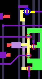
Below is an example of a NOR gate taken from Visual 2A03, related to controlling when the first square channel is silenced:
If any of the gates in red circles are open (high), the current from the highlighted node will go to ground instead of to the gate in the blue circle on the top. Hence the value that reaches the gate in the blue circle is the NOR of the values on the gates in the red circles.
The gate in the blue circle is part of a pass transistor, so called because it passes current between two nodes rather than driving or grounding a node. The gate in this case is apu_clk1, and we say that value is "buffered on apu_clk1".
Storage elements
Cross-coupled inverters
Two cross-coupled inverters will make a latch (an element that stores a single bit). This arrangement is often used for latches that are set or cleared by specific logic rather than by having a value copied into them (from e.g. a data bus line).
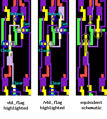
Below is the VBlank flag from Visual 2C02. To the left the vbl_flag node is highlighted, and to the right its inverse is highlighted. (We would label the inverse /vbl_flag, where "/" denotes "inverse" or "active low"). As can be seen by the two gates in white circles, each inverts into the other, forming two cross-coupled inverters.
(The different highlight colors are due to vbl_flag being set when the screenshot was taken.)
The two gates in blue circles set and clear the latch, respectively. To clear the latch, vbl_flag is driven low. To set the latch, /vbl_flag is driven low.
This circuit is an example of an SR Latch, where S stands for set and R for reset, corresponding to the set and clear gates above. It is more specifically an SR NOR Latch, as it can be viewed as being built of NOR gates (where e.g. set together with the upper gate in the white circle constitute a NOR).
Clocked latches
When a latch can be set directly from the value of some line, e.g. a data bus line, an arrangement involving a clock is often used. The motivation is to avoid having to form both data_line and /data_line and route them to the respective terminals of the latch, which would use more logic. (The clock is already routed all around the chip, so mixing it in usually isn't as much of a problem.)
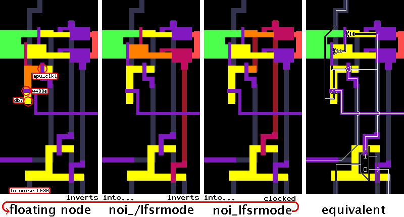
As an example, here's the noi_lfsrmode node (the "Loop noise" flag from $400E):
When apu_clk1 is high, noi_lfsrmode will flow into the second highlighted node, which then inverts into /noi_lfsrmode, forming a cross-coupled inverter latch. While apu_clk1 is low, the loop will be broken momentarily, and during this phase a new value can be copied into the latch by opening the w400e gate (which goes high on writes to $400E). The value let through by the pass transistor is the _db7 node, corresponding to the seventh bit of the data bus. (There's a via between the diffusion and the _db7 line - easier to see if the node is highlighted.) If the loop was not broken during the write operation, the old value in the latch would interfere with setting a new value.
Wire capacitance as storage
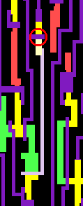
If a wire is "closed off" so that it is no longer connected to neither power nor ground, it will retain its value for a while through capacitance. This is used to store some short-lived data "on the wire" without requiring a latch (this is called dynamic logic, since it has time-dependent behavior beyond just the input clock). As an example, here's the read buffer for the 2C02's VBlank flag, which lets its value be read even though reading $2002 immediately clears the VBlank flag:
When the circled gate (/read_2002_output_vblank_flag) goes low, the gate closes, holding the value. When the circled gate is high, the value of vbl_flag (or rather /vbl_flag in this case) is connected to the wire.
The clocked latch, described above, also makes use of wire capacitance when both the clock and the write enable are low. Chips which make use of this technique tend to have a minimum clock speed at which they can function correctly.
Miscellaneous circuitry
Digital-to-analog conversion
The below Visual 2A03 circuitry controls the volume on the output pin for the two square channels (the triangle, noise, and DMC channels use a separate pin). Note that each successive bit has twice the weight of the preceding one in terms of the amount of powered diffusion connected to it.
Cut-off connections
Some parts of the chips, especially outside the 6502 core, were designed using a copy-and-paste process called "standard cell", leading to some seemingly nonsensical and cut-off connections. These carry no special significance. The image below contains an example. The 6502 core inside the 2A03 is a substantially tighter block of NMOS, but it still has a few cut-off connections remaining from removal of the patented decimal mode.
Layers
(This information is not essential to reading the diagrams.)
The layers that make up the chip are as follows, in order from bottom to top: substrate, diffusion, oxide (with holes for buried contacts and vias), polysilicon, more oxide (with holes for vias), metal, and passivation (or "overglass", containing holes where bond wires connect).
The way diffusion is powered or grounded is through vias to large areas of metal that are either grounded or powered.
Terms
Below are various terms you might run into:
- Buried contact
- A connection between diffusion and polysilicon.
- NMOS
- The technology used for the transistors in the 2A03 and 2C02. In NMOS, transistors are n-doped (have an excess of electrons - the "n" is presumably from the electrons' negative charge). This type of transistor is good at sinking current to ground (this is what causes a 0 bit to usually "win" in bus conflicts), and worse at pulling up. PMOS is the opposite. The transistors used in NMOS and PMOS are sometimes called nMOSFET and pMOSFET, respectively.
- Open drain
- A type of output that works by sinking current from an external pull-up resistor instead of generating current on its own. An example is the PPU's INT pin. The pull-up resistor is denoted "RM1" in this wiring diagram.
- Pull-up resistor
- A resistor connected to power. "Pull-up" comes from pulling the wire to a high state.
- Pull-up transistor
- A transistor whose gate when open causes current to flow from a power source.
- Via
- A connection between polysilicon/diffusion and metal.
Local copies of the simulator
Being able to add node names to nodenames.js can be very helpful when figuring out a circuit. To do this, a local version of the simulator can be downloaded with e.g. $ wget --convert-links on a *nix system. Please watch the recursion level and avoid downloading data needlessly, as at least Visual 2C02 and Visual 2A03 are hosted on a limited uplink.
