Implementing Mappers In Hardware: Difference between revisions
m (→Using 74139 as address decoder and for eliminating bus conflicts: s/regs/resistors) |
m (Kid Dracula italics) |
||
| Line 327: | Line 327: | ||
[[File:Kid dracula scanline.png]] | [[File:Kid dracula scanline.png]] | ||
Source: Kid Dracula pirate famicom cart, See also: https://forums.nesdev.org/viewtopic.php?f=9&t=15302 | Source: ''Kid Dracula'' pirate famicom cart, See also: https://forums.nesdev.org/viewtopic.php?f=9&t=15302 | ||
See also: https://forums.nesdev.org/viewtopic.php?f=9&t=9283 | See also: https://forums.nesdev.org/viewtopic.php?f=9&t=9283 | ||
Revision as of 19:35, 13 February 2023
With increased popularity of programmable logic devices (CPLD/FPGA), almost any mapper implementation can be done in just one chip with some additional components for:
- logic level translating (5 V from cart connector signal to 3.3 V),
- recovering !RESET signal from M2,
- protecting PRG-RAM against data corruption due to PRG-!CE and M2 delay,
- battery backing-up PRG-RAM,
- providing additional audio channels (AY-8910 or similar chips).
However, most CPLD/FPGA chips come in dense packages, which makes soldering them hard for beginners. Also, they need 2.5 V and/or 3.3 V power supply and logic levels-translators, which might discourage using them for simple mapper reproduction. Learning how to implement some mappers using discrete chips (74 and 40 family) might be more economical for some uses. Also, it is good educational exercise for understanding:
- how console works and how to interact with CPU and PPU on hardware level,
- which signals need to be used and how much resources it would take to express the same in programmable logic devices.
A lot of bootleg (pirate) cart reproductions were done using 74 and 40 families chips, because that was the only way to mimic the behavior of ASIC mappers like MMC1 or MMC3 at that time.
This page shows some tricks and solutions for common problems during implementing logic using discrete circuits. Exclamation mark placed at beginning of signal names makes them active low (inverted logic) - for example: !OE or CPU_R/!W
5V CMOS Versus 5V TTL
Before starting to build something using discrete chips, it is important to realize that TTL outputs can not drive CMOS inputs. Given a VCC of 5.0V, a TTL output high (VOH) is typically 3.3V, and a CMOS input high (VIH) is typically 3.7V. Here are the typical thresholds when Vcc = 5.0V[1]:
| Technology | Output High (VOH) | Input High (VIH) | Input Low (VIL) | Output Low (VOL) |
|---|---|---|---|---|
| CMOS (74HCxx, 74AHCxx, CD40xx) | 4.7V | 3.7V | 1.3V | 0.2V |
| TTL-Compatible-CMOS (74HCTxx, 74ACTxx) | 4.7V | 2.0V | 0.8V | 0.2V |
| TTL (74LSxx, 74Sxx, 74Fxx) | 3.3V | 2.0V | 0.8V | 0.35V |
In general:
- TTL-Compatible-CMOS can work with anything.
- CMOS outputs can drive TTL inputs.
- TTL outputs can NOT drive CMOS inputs.
Also be advised, that when using CMOS chips, you should place a ceramic bypass capacitor close to power supply pins of every chip. An ordinary 100 nF ceramic capacitor is ideal for this purpose. There should also be a larger capacitor from VCC to GND for the whole cartridge. This would typically be an electrolytic capacitor of 10 uF. Finally, all unused inputs of CMOS devices should be tied to some known state (GND, VCC or any other signal). In contrast, TTL unused inputs can be left unconnected without any harm. An unconnected TTL input will have logic value of '1'.
Combining ASICs and discrete logic also need notice this, for example, when inverting the WRAMCE of AX5904, 74LS04 works, 74LVC1G04 not.
5V Versus 3.3V
Modern ICs, especially memories, CPLDs, and FPGAs, tend to run on 3.3V CMOS logic instead of the 5V CMOS/TTL logic native to the Famicom/NES. In order to use these parts, one must create a 3.3V power rail to power them. The part selected must either have 5V-tolerant digital I/Os, or one must employ a method of level-shifting. Beware that some parts that advertise 5V tolerant I/O actually require additional external components to complete the internal level shifting circuits.
Generating a 3.3V Power Rail
              ______________
5V Rail ---+->|IN       OUT|--+-------> 3.3V Rail
           |  | LM1117-3.3 |  |
     10 uF =  |____________|  = 10 uF
           |        |         |
    GND ---+--------+---------+-------- GND
To generate 3.3V, simply use a small and inexpensive 3.3V linear voltage regulator, such as LM1117-3.3. It is not a great idea to use a zener diode, LED, resistor divider, or any other tricks like that.
Level Shifting 5V Output For 3.3V Input
The main thing to consider here is if the 5V output high can exceed the maximum input voltage of the 3.3V input. If so, something needs to go in between that knocks down the voltage.
Series Resistor
5V Output ---/\/\/--- 3.3V Input
Much better than nothing, but not recommended. This is basically the same as "Resistor + Clamp Diode" below, relying on an internal clamp diode on the 3.3V input. These diodes are designed for ESD protection and may open or short over time when used like this. Only use this circuit if the datasheet says so, or if there isn't a better alternative.
Resistor Divider
5V Output ---/\/\/---+----------- 3.3V Input
                     |
                     +---/\/\/--- GND
Pretty basic, just divide it down to bring the voltage in range while not overloading the output current. Since the output and input impedances are basically uncontrolled, this method is pretty sketchy and is probably subject to dynamic behaviors, including internal capacitance on the 3.3V input. But in theory it could work.
Resistor + Clamp Diode
                     +---►|--- 3.3V
                     |
5V Output ---/\/\/---+-------- 3.3V Input
This common method uses a diode to clamp the signal. Note that the diode has a voltage drop of 0.4-0.7V, depending on the type of diode selected. The 3.3V input will see a maximum of the clamp voltage (3.3V) + the diode drop (0.4V Schottky) = 3.7V. Also to consider: Does your 3.3V rail have the ability to dissipate enough energy not to be "pushed up" by this diode? It may make sense to generate an additional 2.9V or 3.0V rail with a zener diode, and direct the diode to that rail. The zener would then hold the rail very firmly from floating up. Alternatively, one could add a resistor from the 3.3V rail to GND. This would load it and help prevent it from floating up.
74LV, 74LVC, 74LVCT Series
             |\
5V Output ---| >--- 3.3V Input
             |/
These digital logic chips are designed to run on a 3.3V rail, have 3.3V CMOS outputs, and accept 5V inputs. Hex buffers are available. These are a really great solution for shifting 5V outputs for 3.3V inputs. They come in various packages including DIP, SOIC, and SSOP. These can also be used to implement a mapper and level shift at the same time.
Level Shifting 3.3V Output For 5V Input
If we could trust that digital inputs are all high-impedance, a 3.3V digital output could be considered quite similar to a 5V TTL output in terms of output logic levels. However, TTL inputs are internally pulled high. So in effect, you may be pulling a 3.3V output up to 5V. It isn't entirely clear if that is safe or not.
Clamp Diode
                       +---►|--- 3.3V
                       |
3.3V Output -----------+-------- 5V TTL Input
Same comments apply as when using a clamp diode in the other shifting direction. This circuit prevents a TTL 5V input from pulling the 3.3V output too high.
74HCT, 74ACT Series
These digital logic chips are designed to run on a 5V rail, have 5V CMOS outputs, and accept 5V TTL inputs. In theory, the ability to accept a TTL input would suggest that it could accept a 3.3V input, since that is a very similar logic high threshold to 5V TTL.
Level Shifting Bidirectional Between 3.3V and 5V
The CPU and PPU data busses of the Famicom/NES go both directions, so level shifting must go both ways in this case. It creates additional challenges.
Automatic Bidirectional Level Shifters
    3.3V ---+---+  2N7000    +----- 5V
            <   |_______     <
        10k >    -  -  -     > 10k
            <    |  ▲  |     <
3.3V I/O ---+----+--+  +-----+----- 5V I/O
Automatic level shifters exist that don't need to be told the direction. They are made from a FET and two resistors. Small pre-built PCBs that do this are available. These reportedly do not work with the speed and reliability needed for the Famicom/NES. These should be avoided.
Similar: TXB0108, NTS0308E. It is unknown if these particular chips are suitable for level shifting Famicom data busses. These are potentially a really great, simple solution if they can be shown to be reliable for this application.
74LVC245
This particular chip is an octal bus transceiver that sits on the 3.3V rail. It has 5V-tolerant inputs, and its outputs are 3.3V, which make it appear as a 5V TTL output. It has 2 additional inputs: DIR, sets the direction, and /E disconnects everything when high. DIR and /E must be logically controlled, which does present challenges. For the CPU data bus, using /ROMSEL and CPU R/W alone is not adequate when accessing memory locations below $8000 in the cartridge. These accesses may be required for PRG-RAM or mapper registers, depending on the mapper. Open-bus behaviors are affected by this approach. Signal timings must be considered. Similar challenges are faced for the PPU data bus.
This method can not drive 5V CMOS. For this, you may want the 74LVC4245 instead (note the extra 4). Or to reduce component count, consider 74ALVC164245, which translates two 8-bit buses at once.
Dual 3-State Buffers
Basically building the two halves of the 74LVC245 separately, you are then free to mix logic families with all the single-direction options. For example, 74LVC244 powered by 3.3V can take in 5V TTL/CMOS inputs, and put out 3.3V logic. 74HCT244 powered by 5V can take in 3.3V inputs, and put out 5V CMOS logic. Additional logic to run the 3-state operation of each chip. This solution uses numerous chips.
Recovering !RESET signal from M2
Most CPLD/FPGA chips can be programmed in a way that their internal registers have predefined value upon power-up. In contrary, 74XX chips have unknown (random) internal state and they need to be put to reset after power-up for a while. There is no !RESET signal on the cartridge edge, but M2 CPU clock signal (which is oscillating at ≈ 1.8 MHz during normal work and is held in high impedance when CPU is being reset) can be used for that purpose. The following circuit recovers !RESET from M2:
         VCC
          |
          C (1n)
          |
M2---►|---+----- `recovered` !RESET
          |       ('0' when console is in reset)
          R (4.7k)
          |
         GND
When M2 is oscillating, there is:
- '1' at output (when M2 is '1') because C is discharged through the diode,
- '1' at output (when M2 is '0') because diode protects !RESET from dropping to '0', but C is slowly charged through R.
When M2 stops oscillating for a longer period of time (high impedance state or '0'), C will be charged through R and the voltage at output will be slowly falling and finally it will reach '0' level. Manipulating R*C can shorten or lengthen that period.
Pros:
- Can be used as asynchronous reset for both 7400 family and FPGA devices.
Cons:
- The signal at the output has slow rise time and cannot be used as a clock to sequential logic (for example, when you want to switch to next game in your multi-cart after each reset), because it might produce multiple oscillations during its rising and falling edge. Solution: put additional Schmitt gate (eg. 7414) at such sequential logic input:
                           _
                          | \
`recovered` reset---------|S >------input to seqiential logic
                          |_/
Source: 168-in-1 (and almost any other) multicart.
Using high-impedance + pull up for last-fixed bank
Normally, when you want to make some CPU memory region (eg. $C000-$FFFF like in UNROM) to be fixed to the last bank, you should OR the PRG address lines with CPU-A14:
 REGISTER
|------------+                   ____
|      bit0  |------------------) OR )------PRG_A14
|            |          CPU_A14-)____)
|            |                   ____
|      bit1  |------------------) OR )------PRG_A15
|            |          CPU_A14-)____)
|            |                   ____
|      bit2  |------------------) OR )------PRG_A16
|------------+          CPU_A14-)____)
If you want to eliminate need of using OR gate and your REGISTER has three-state outputs, you can pull-up its output to VCC so that when they're disabled, all PRG lines are fixed to '1'. Instead of using discrete resistors, you can use pull-up ladder (R can be 10k)
                                  VCC VCC VCC
           REGISTER                |   |   |
          +------------+           R   R   R
          |      bit0  |-----------+-----------PRG_A14
          |            |               |   |
          |            |               |   |
          |      bit1  |---------------+-------PRG_A15
          |            |                   |
          |            |                   |
          |      bit2  |-------------------+---PRG_A16
          |            |
CPU_A14---| !OE        |
          +------------+
Pros:
- allow you to save one chip,
- might make routing signals easier
Cons:
- '0' to '1' transition edge (switching output off) is slower, because external capacitance is preloaded through large R. However, it should not cause problems as most of memories are 200 ns or less. You can speed the edge up by lowering R value
Source: Sangokushi 2 pirate MMC5 bootleg
Using 74139 as address decoder and for eliminating bus conflicts
When you want to implement something with more than one register (or one register but not placing it in whole $8000-$ffff), you need some kind of address-decoding circuitry which takes A14, CPU_R/!W and maybe other lines into account. Also, eliminating bus conflicts also needs to take CPU_R/!W into account which might need of use lot of combinatorial logic.
74139 which is two 4-to-2 decoder can be used to both decode address and as some way of combinatorial logic. For example, implementing Camerica 71 mapper (single reg placed at $C000-$FFFF + no bus conflict) would need only 74574 register + 74139 decoder + pull-up resistors:
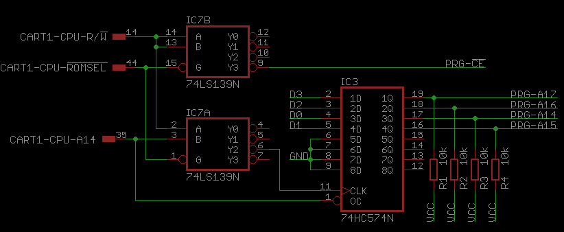
Source: my own work
Protect registers from accidental writing
When you are making multi-cart, you will probably have to create some registers for selecting games (PRG and CHR), mirroring and put them in $8000-$ffff. But when the user selects game and you do JMP ($fffc), you don't know whether the game doesn't also write to $8000-$ffff, which might change currently selected bank and contribute to CPU hang. To protect against that situation, you need to block any succesive writes to $8000-$ffff from changing currently stored value in yours register. Easiest solution is to make one bit of your register as a LOCK BIT and then OR it with original register write strobe. When LOCK BIT is '1', affective register write strobe will remain '1' no matter what happens (until CPU reset). Don't forget to clear this bit (or whole register) on CPU reset.
                                                           __________
                                                          | REGISTER |
                                            DATA         -|          |---- TO PRG_A/CHR_A
                                            and/or       -|          |---- or other logic
                                            ADDRESS bus  -|LOCK BIT  |-+
               _________________________            __    |          | |
--signals-----| combinatorial logic for |--+-------)OR)---|wr clock  | |
--from cart---| generating register     |  |     +-)__)   |__________| |
--edge--------| write strobe            |  C     |                     |
              |_________________________|  |     +---------------------+
                                          GND
Notes:
- C (tens or hundreds of pF) might be useful if not all input signals change at the same time to prevent short glitches at output.
Source: 4-in-1 multicart
Protect CHR-RAM from being overwritten
If you plan to make flash-cart or reproduction, but instead of using CHR-ROM you want to use CHR-RAM and fill its pattern tables through PPUADDR/PPUDATA, it is OK. However, there are some games, which are designed to be using CHR-ROM but they're still forcing PPU to write something to $0000-$1FFF, which cause overwriting some tiles. To protect against that, you should make one bit of your register as CHR_RAM_LOCK bit:
 ______________
| REGISTER     |                          CHR_RAM
|              |              __           _______
|CHR_RAM_LOCK  |-------------)OR)_________|!CS
|              |    PPU_A13--)__)         |
|______________|                 PPU_!RD--|!OE
                                 PPU_!WR--|!WE
                                          |_______
One could also use Flash memory for CHR and reprogram it before starting the game. In that case, its native protection against spurious writes could be used instead. However, the time to reprogram the Flash could become objectionable.
Source: 168-in-1 multicart (it does something like that although it uses PAL circuitry for combinatorial logic)
Building complicated logic formulas
When constructing complicated logic expressions (eg. address decoders), you might need a lot of AND/NAND/OR/NOR/EXOR gates to build them. Theoretically, all logic formulas can be build using only NAND gates, but sometimes you would need so many of them it would be really impractical. 74688 is a 8-bit comparator (with additional output enable) which might be extremely useful for address decoding purposes. If you want to build even more complicated decoders, you can:
- use some kind of programmable logic (PAL, GAL, CPLD). Although, the first two are rather hard to find and program,
- use EPROM/Flash as a cheap-man's PLD. A memory with address bus of width `n` and data bus of width `m` can be used to build ANY `n` input and `m` output combinatoric logic. It can also be used to build sequential logic (when connecting data outputs to address inputs), but you need to be aware of transient states to make it work.
Source: http://hackaday.com/2017/02/02/the-gray-1-a-computer-composed-entirely-of-rom-and-ram/
Implementing lot of registers using 74670 dual port memory
A lot of mappers have more than one register (for example - MMC3 has 8 registers just for controlling CHR banks). Theoretically, you can implement every register as 74574/74373 or any other n-bit latch + some circuitry for decoding writing signals to them (74138) and a lot of demultiplexers, but that would be pain in designing and routing the PCB.
74670 (4 x 4 register file) is a dual-port memory which has 4 memory cells, each 4 bits width. There are two lines for selecting cell to read and another two lines for selecting cell to write. You can connect those chips in parallel to widen data bus or in series (plus address decoder) to widen address bus.
Source: Sangokushi 2 pirate MMC5 bootleg, Super Mario Bros 3 (?) pirate MMC3 bootleg
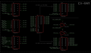
Implementing dual port EXRAM (like in MMC5)
MMC5 is one of the most complex mapper in terms of functionality and number of logic cells if would take to implement it. Not many games were created on it because it appeared really late. Koei used it with passion in their games, probably because if game used EXRAM, it would be nearly impossible to clone it without MMC5 chip. Using SRAM + 74157 (as address bus multiplexer) + 74245 (as data buss buffer) and some additional logic for controlling them is all you need for adding EXRAM support.
Source: Sangokushi 2 pirate MMC5 bootleg
Multiplexers
74153 (dual 4-line to 1-Line Data Selectors/Multiplexers) is one of the most frequently used multiplexer in discrete cartridges. However, its most frequent use is by dividing it into two separate 2-line to 1-line multiplexer. Most often, first part is for controlling banking size and second part is for changing type of mirroring.
Source: 150-in-1 multicart
Widening registers
The most frequent width of registers are:
- 8 bit (74574/74373 latch),
- 6 bit (74174)
- 4 bit (74161),
- 1 bit (7474).
The last one is most universal because it consist of two separate RS flip-flops. If you want to create register with odd width (for example: 5 or 9), you can mix those chips and connect them in parallel (connect their write clocks together).
Serial to parallel conversion
When you want to receive serial stream of bits and store it in parallel register, you will have to use some kind of shift register. 4015 (Dual 4-Stage Static Shift Register) can be used as shown below to receive 9 bit of keyboard serial data stream:
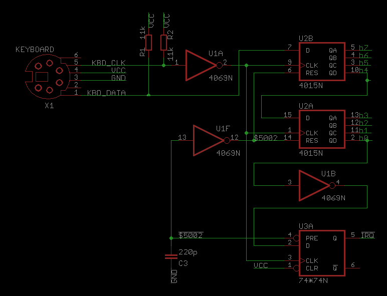
Source: Dendy Keyboard Transformer cart
Mirroring switch
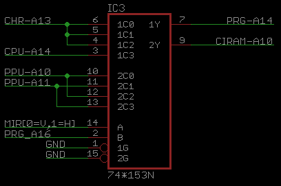
Mirroring switch can be also implemented using NAND gates like below with the formula: CIRAM_A10 = !(!(PA10 & MIRR) & !(!MIR & PA11))
Proof:
when MIRR='0': CIRAM_A10 = !(!(PA10 & 0) & !(1 & PA11)) = !(1 & !PA11) = PA11 = H
when MIRR='1': CIRAM_A10 = !(!(PA10 & 1) & !(0 & PA11)) = !(!PA10 & 1) = PA10 = V

Example (among many others): Holy Diver
Cycle counter and interrupt notification
Cycle counter and interrupt notification are rare features of discrete mappers, because they need quite a lot of chips. Things that can be counted are: video scanlines, CPU cycles or PPU cycles. Scanline counting is useful for notifying via interrupt about incoming scanline in order to switch nametables and/or CHR banks. The main use is to generate complex graphics that uses more than 256 tiles per screen or status bars. Schematics for the whole thing might be like below:
              ___________            ______________
             |           |          |              |
  PPU_A12 ---| clock     |----------|CLK  counter  |-+
             | generator | +------+-|RST           | |  ____________     ______________
             |___________| |        |______________| +-|            |   |interrupt     |
                           |         ______________    | comparator |---|generation and|---!IRQ
                           |        | register for   +-|____________|   |acknowledgment|
                           |        | storing      | |                  |______________|
                           | CPU_D--| compared val |-+                       |
                           |      +-|______________|                         |
                           |      |                                          |
              _________    |      |                                          |
           --| address |---+      |                                          |
           --| decoder |----------+                                          |
           --|_________|-----------------------------------------------------+
- Counter clock generator - something to clock you counter. If you plan to count scanlines, you can connect PPU_A12 as a clock, like in MMC3, but don't forget that this line oscillates 8 time every scanline so your counter will be incremented by 8 every line, unless you add something to ignore close edges. 220pF cap to GND might be useful to eliminate short glitches. Other option might be to use M2 as clock (to count CPU cycles, line in Mapper 90 or 69)
- The counter itself - something like 74*161 (4 bit counter with), 74*393 (two 4 bit counters)
- Register for storing compared value - if your game wants to set at which scanline the interrupt should be fired. This block can be skipped if interrupt should be fired at fixed counter value.
- Comparator - to compare counter counter value against stored value,
- Interrupt generation and acknowledgment - for disabling/enabling interrupt generation and acknowleding pending interrupts.
- address decoder - generating enable signals for each of the blocks above on the basis of CPU address
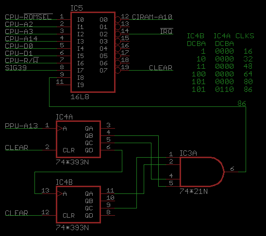
In the schematics below, there is some logic which counts PPU scanlines. PAL16L8 is used for address decoder & interrupt generation and acknowledgment. This circuit counts 86 falling edges of PPU A13, or 2 scanlines with a horizontal precision of 8 pixels from when it was started.
Source: Kid Dracula pirate famicom cart, See also: https://forums.nesdev.org/viewtopic.php?f=9&t=15302
See also: https://forums.nesdev.org/viewtopic.php?f=9&t=9283
