Game Genie: Difference between revisions
m (Fixes typos and improves syntax.) |
(→External links: updated link to Kevin Selwyn's disassembly post) |
||
| Line 91: | Line 91: | ||
== External links == | == External links == | ||
* [ | * [https://www.kevinselwyn.com/posts/game-genie-disassembly/ NES Game Genie ROM disassembly] by Kevin Selwyn ([http://github.com/kevinselwyn/game-genie-disassembly GitHub page]) | ||
* [http://github.com/qalle2/nes-gg-disassembly NES Game Genie ROM disassembly] by qalle | * [http://github.com/qalle2/nes-gg-disassembly NES Game Genie ROM disassembly] by qalle | ||
Revision as of 10:49, 31 December 2021
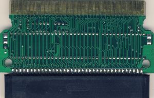
The Game Genie is a enhancement cart for the NES designed by Camerica and distributed by Galoob and Camerica. It functions as a pass-thru, with a 72-pin cartridge connector connecting it to the NES, and a 72-pin cartridge slot for a game to be inserted into. When plugged in between a game and the NES and turned on, it provides a simple interface to enter up to three cheat codes, which then modify the behavior of the game. First revision were build using ASIC blob chip and 4 kB ROM, the latter one has both chips integrated into single epoxy blob. There even exist a console (Geniecom Enhance Console video Game) that has the Game Genie ASIC DIP CHIP (GENIECOM-V1 BIC) built it.
The Game Genie is not assigned a mapper number.
Technical
The Game Genie works by intercepting CPU reads and replacing the game cart's response with its own response. It can intercept any three addresses in CPU $8000…$FFFF and respond with a single replacement for each. To make the tool more compatible with bank-switching, each of the three codes has an optional compare value which can be used to only replace the byte if the original byte matches the compare, hopefully limiting the cheat to functioning on the desired bank.
When first booted, the Game Genie presents its own 4-KiB PRG ROM and a series of simple gates masquerading as a CHR ROM. The included PRG ROM runs code to show a simple code entry user interface. When the user presses Start, the cheat values are written to memory-mapped registers, and then another register is written which switches the Game Genie into game mode, where the attached game cart's CHR and PRG is passed through, save whatever code replacements were defined. The Game Genie remains in game mode until power-cycled, and will respond to no further writes.
Registers
Master Control ($8000)
7  bit  0
---- ----
.DDD CCCE
 ||| ||||
 ||| |||+- Write 1 to switch into game mode
 ||| +++-- Compare enable for each of the three codes
 +++------ Disable each of the three codes
Bit 1 and 4 correspond to the code at $8001…$8004.
Game Genie writes first a value with bit 0 set and then writes 0x00 to this register. Because after the first write, the GameGenie logic switches into game mode, any further writes to range $8000-$ffff will cause the slave cartridge /ROMSEL to become low for that write cycle. As a result, the second write will be seen and interpreted by the hardware inside slave game cartridge. The reason for this write is unknown, maybe it initializes the bank select register for MMC3 games?
Address High ($8001, $8005, $8009)
7  bit  0
---- ----
.AAA AAAA
 ||| ||||
 +++-++++- Bits 8:14 of address for this cheat (Bit 15 fixed to 1)
Address Low ($8002, $8006, $800A)
7  bit  0
---- ----
AAAA AAAA
|||| ||||
++++-++++- Bits 0:7 of address for this cheat
Compare ($8003, $8007, $800B)
7  bit  0
---- ----
CCCC CCCC
|||| ||||
++++-++++- Compare value for this cheat (write 0 if unused?)
Replace ($8004, $8008, $800C)
7  bit  0
---- ----
RRRR RRRR
|||| ||||
++++-++++- Replacement value for this cheat
Unknown ($FFF0, $FFF1)
The Game Genie rom writes 0 to $FFF0, $FFF1, $FFF0 in that sequence.
Pattern Tables
When game mode is inactive, the Game Genie generates PPU pattern tables through PPU $0000…$1FFF by the following method:
- When PPU A2 = 1:
- PPU A4 → PPU D4…D7
- PPU A5 → PPU D0…D3
- When PPU A2 = 0:
- PPU A6 → PPU D4…D7
- PPU A7 → PPU D0…D3
This creates 16 distinct objects that are used to build the menu graphics:
Bugs
Because of how the hardware is designed, there are some bugs or limitations of this device
- When a cartridge has something mapped at $4020-$7FFF (WRAM, PRG ROM) and a code for region $C020-$FFFF is added, the Game Genie will hold the slave cartridge's /ROMSEL at 1 when reading from that location. But then, the cartridge logic will see this read cycle as something below $8000, enabling the chip that is mapped here, causing bus conflict at this location and resulting in invalid data being returned to the CPU. [1]
- Cartridges that rely only on PPU /A13 when decoding CHR-ROM (like MMC5) will not display the the Game Genie menu properly, as the Game Genie ignores this line, causing bus conflict.
- According to the Game Genie patent, the process of determining if a code with comparison should be enabled is asynchronous. This makes it impossible to apply multiple codes with the same address but different replace/compare values. The Game Genie allows entering such codes, but when it comes to sending them to the ASIC chip, only the first such code will be enabled.
References
- nesgg.txt – NES Game Genie Code Format DOC v0.71 by Benzene of Digital Emutations, 1997-07-10
- Patent US5112051A – Interfacing device for a computer games system
External links
- NES Game Genie ROM disassembly by Kevin Selwyn (GitHub page)
- NES Game Genie ROM disassembly by qalle


