Visual circuit tutorial: Difference between revisions
mNo edit summary |
mNo edit summary |
||
| Line 176: | Line 176: | ||
Note that this is ''not'' an instance of cross-coupled inverters, as neither node is directly connected to a power source. Rather, DRAM depends on capacitance to hold the value, which will fade unless the capacitor is regularly ''refreshed'' (the high side recharged). (This is the "dynamic" part of DRAM.) | Note that this is ''not'' an instance of cross-coupled inverters, as neither node is directly connected to a power source. Rather, DRAM depends on capacitance to hold the value, which will fade unless the capacitor is regularly ''refreshed'' (the high side recharged). (This is the "dynamic" part of DRAM.) | ||
'''TODO: Work in progress''' | '''TODO: Work in progress. More text and pictures coming tomorrow, so additions might get lost.''' | ||
== Miscellaneous circuitry == | == Miscellaneous circuitry == | ||
Revision as of 12:05, 28 May 2013
This is a crash course on making sense of the circuit displays in Visual 6502/2C02/2A03, written for people without much low-level electronics experience (like the author). It aims to present the information needed to read the diagrams at a basic level in simple language, omitting details that are unimportant when starting out.
You might want to read the Visual 6502 user's guide and the Visual 2C02 page first.
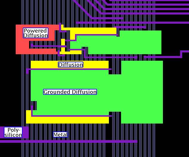
What the different colored areas are
Let's start by defining what the different colors mean:
- Green areas are diffusion (explained below) connected to ground.
- Red areas are diffusion connected to VCC (power).
- Yellow areas are diffusion that is neither connected directly to ground nor directly to VCC.
- Gray areas are metal.
- Purple areas are polysilicon (often shortened to just "poly").
At the level presented here, diffusion, metal, and polysilicon can be thought of as roughly equivalent when viewed in isolation; they all conduct current. The important difference is in how they interact with each other, which is explained below.
Basic building blocks
Transistors
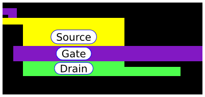
When a piece of polysilicon is sandwiched between two areas of diffusion, it acts as a gate, only letting current through when the polysilicon is powered (or, equivalently, high, 1, or open). The diffusion area from which current will flow when the gate is open is called the source. The diffusion area into which current will flow is called the drain. The gate together with the source and drain is what makes a transistor.
Power sources
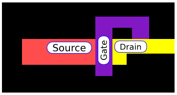
Around an area of powered diffusion we will often see something like the following (note the distinctive "hook" in the polysilicon):
Here the polysilicon acts roughly like a resistor, preventing a short from VCC to ground when the power source would otherwise have a direct connection to ground along some path of open gates.
Nodes
Electrically common areas are called nodes in Visual 6502/2C02/2A03. Clicking on a node will highlight it, making it easier to see how things are connected (clicking on powered or grounded diffusion won't work; these only modify properties of other nodes and are not themselves nodes). When a node is highlighted, a numeric ID unique to the node will be displayed in the upper right, along with a name for the node if it has one. Node names are defined in nodenames.js.
Transistors can be selected separately by clicking on the gate (the part of the polysilicon between the diffusion areas). They have names that start with "t", followed by a numeric ID.
The Find: edit field can be used to locate nodes, either by numeric ID or by name. Numeric IDs can also be used to trace the values of nodes without an assigned name.
Logic elements
Inverters
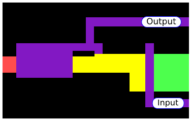
An inverter is constructed like in the image below:
When the input gate is low, current flows into the output wire. When the input gate is high, current flows into ground, driving the output wire low. The output wire is hence the inverse of the input wire.
When one node is the inverse of another, it is said that it inverts into the other node.
NOR gates
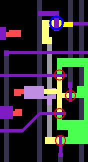
Below is an example of a NOR gate taken from Visual 2A03, related to controlling when the first square channel is silenced:
If any of the gates in red circles are open (high), the current from the highlighted node will go to ground instead of to the gate in the blue circle on the top. Hence the value that reaches the gate in the blue circle is the NOR of the values on the gates in the red circles.
The gate in the blue circle is part of a pass transistor, so called because it passes current between two nodes rather than driving or grounding a node. The gate in this case is apu_clk1, and we say that value is "buffered on apu_clk1".
Storage elements
Cross-coupled inverters
Two cross-coupled inverters will make a latch (an element that stores a single bit). This arrangement is often used for latches that are set or cleared by specific logic rather than by having a value copied into them (from e.g. a data bus line).
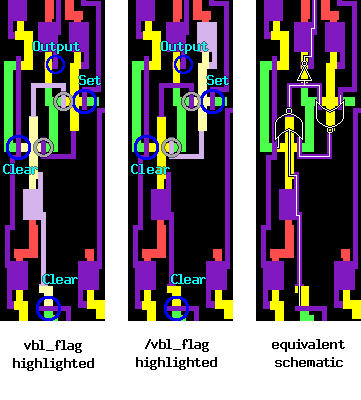
Below is the VBlank flag from Visual 2C02. To the left the vbl_flag node is highlighted, and to the right its inverse is highlighted. (We would label the inverse /vbl_flag, where "/" denotes "inverse" or "active low"). As can be seen by the two gates in white circles, each inverts into the other, forming two cross-coupled inverters.
(The different highlight colors are due to vbl_flag being set when the screenshot was taken.)
The two gates in blue circles set and clear the latch, respectively. To clear the latch, vbl_flag is driven low. To set the latch, /vbl_flag is driven low.
This circuit is an example of an SR Latch, where S stands for set and R for reset, corresponding to the set and clear gates above. It is more specifically an SR NOR Latch, as it can be viewed as being built of NOR gates (where e.g. set together with the upper gate in the white circle constitute a NOR).
Clocked latches
When a latch can be set directly from the value of some line, e.g. a data bus line, an arrangement involving a clock is often used. The motivation is to avoid having to form both data_line and /data_line and route them to the respective terminals of the latch, which would use more logic. (The clock is already routed all around the chip, so mixing it in usually isn't as much of a problem.)
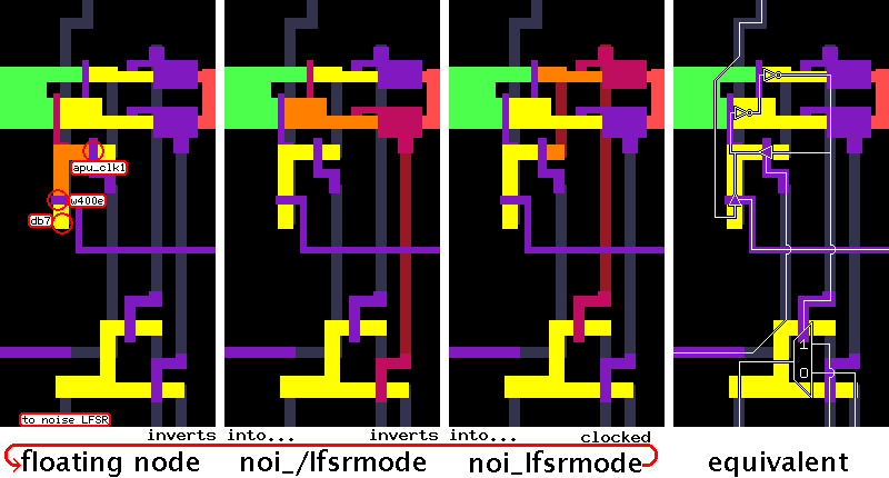
As an example, here's the noi_lfsrmode node (the "Loop noise" flag from $400E):
When apu_clk1 is high, noi_lfsrmode will flow into the second highlighted node, which then inverts into /noi_lfsrmode, forming a cross-coupled inverter latch. While apu_clk1 is low, the loop will be broken momentarily, and during this phase a new value can be copied into the latch by opening the w400e gate (which goes high on writes to $400E). The value let through by the pass transistor is the _db7 node, corresponding to the seventh bit of the data bus. (There's a via between the diffusion and the metal _db7 line - easier to see if the node is highlighted.) If the loop was not broken during the write operation, the old value in the latch would interfere with setting a new value.
Wire capacitance as storage
If a wire is "closed off" so that it is no longer connected to neither power nor ground, it will retain its value for a while through capacitance. This is used to store some short-lived data "on the wire" without requiring a latch (this is called dynamic logic, since it has time-dependent behavior beyond just the input clock). As an example, here's the read buffer for the 2C02's VBlank flag, which lets its value be read even though reading $2002 immediately clears the VBlank flag:
When the circled gate (/read_2002_output_vblank_flag) goes low, the gate closes, holding the value. When the circled gate is high, the value of vbl_flag (or rather /vbl_flag in this case) is connected to the wire.
The clocked latch, described above, also makes use of wire capacitance when both the clock and the write enable are low. Chips which make use of this technique tend to have a minimum clock speed at which they can function correctly.
DRAM (Dynamic RAM)
Below is an example of a DRAM cell, taken from the internal PPU OAM memory:
In the left picture one side of the cell is highlighted, and in the right picture the other side (with different highlight colors due to the node being high in this case). The node highlighted in the left picture corresponds to the value held in the cell (low for 0 and high for 1), and the two nodes are always inverses of each other.
Note that this is not an instance of cross-coupled inverters, as neither node is directly connected to a power source. Rather, DRAM depends on capacitance to hold the value, which will fade unless the capacitor is regularly refreshed (the high side recharged). (This is the "dynamic" part of DRAM.)
TODO: Work in progress. More text and pictures coming tomorrow, so additions might get lost.
Miscellaneous circuitry
Digital-to-analog conversion (DAC)
The below Visual 2A03 circuitry controls the volume on the output pin for the two square channels (the triangle, noise, and DMC channels use a separate pin). Note that each successive bit has twice the weight of the preceding one in terms of the amount of powered diffusion connected to it.
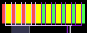
This is an example of a binary-weighted DAC. A different type of DAC is used for the video output from the PPU (found in the upper-left of Visual 2C02, rotated 90 degrees here):
The upper-left end is actually connected to VCC, and the lower-right to ground. This is a resistor ladder, and works by tapping the wire at different points along the run to get different voltages. As the simulator is purely digital, this circuit is not directly used in the simulation, and some parts that would otherwise interfere with it have been disconnected.
Output drivers
These are found on pins capable of doing output, which need to be able to source (generate) and sink large currents to drive the line high or low. Large clusters of pull-up and pull-down transistors like these are sometimes called superbuffers. The polysilicon wire that would cause the pin to source current is highlighted below.
Cut-off connections
Some parts of the chips, especially outside the 6502 core, were designed using a copy-and-paste process called "standard cell", leading to some seemingly nonsensical and cut-off connections. These carry no special significance. The image below contains an example. The 6502 core inside the 2A03 is a substantially tighter block of NMOS, but it still has a few cut-off connections remaining from removal of the patented decimal mode.
Layers
(This information is not essential to reading the diagrams.)
The layers that make up the chip are as follows, in order from bottom to top: substrate, diffusion, oxide (with holes for buried contacts and vias), polysilicon, more oxide (with holes for vias), metal, and passivation (or "overglass", containing holes where bond wires connect).
The way diffusion is powered or grounded is through vias to large areas of metal that are either grounded or powered.
Clocks
This section lists node names for various clocks that sequence operations within the chips. Some of the 6502 pin signals might have gained a "c_" prefix in Visual 2A03 compared to Visual 6502.
6502 core pins
- clk0
- The φ0 clock input pin. Goes low at the beginning of a CPU cycle.
- clk1out, clk2out
- The φ1 and φ2 output pins. φ2 is used to form M2 in the 2A03, which has a modified duty cycle.
6502 internal clock signals
- cp1
- High during the first phase (half-cycle) of a CPU cycle. The inverse of clk0.
- cclk
- High during the second phase of a CPU cycle. Roughly equivalent to clk0, but modified slightly to never overlap with cp1 (though that won't be visible in the simulators).
APU clock signals
- apu_clk1
- This clock signal has a 25% duty cycle. It ticks at half the rate of the CPU clock, and is high only when φ2 is low.
- apu_/clk2
- Like apu_clk1, but ticks on the opposite phase, and is also inverted so that it has a 75% duty cycle.
This clock arrangement helps to ensure that timed events (various counters being decremented or reloaded) do not conflict with writes from the CPU (which only happen when φ2 is high).
| φ1 | 1 | 0 | 1 | 0 | 1 | 0 | 1 | 0 |
|---|---|---|---|---|---|---|---|---|
| φ2 | 0 | 1 | 0 | 1 | 0 | 1 | 0 | 1 |
| apu_clk1 | 1 | 0 | 0 | 0 | 1 | 0 | 0 | 0 |
| apu_/clk2 | 1 | 1 | 0 | 1 | 1 | 1 | 0 | 1 |
PPU clock signals
- clk0
- The input clock, fed from the master clock. Used directly in video waveform generation.
- _clk0
- The inverse of clk0.
- pclk0
- The pixel clock. Derived from clk0 by dividing by four (NTSC) or five (PAL). One cycle corresponds to a rendered dot, with pclk0 being high during the first phase (half-cycle).
- pclk1
- The inverse of pclk0. High during the second phase of a pixel clock.
Terms
Below are various terms you might run into:
- Bond wire
- A wire that connects an internal pad to an external pin on the chip package; see e.g. [1].
- Buried contact
- A connection between diffusion and polysilicon.
- NMOS
- The technology used for the transistors in the 2A03 and 2C02. In NMOS, transistors are made by creating regions of n-doped semiconductor that become the source and drain ("n-doped" because this doping increases the mobility of electrons and their negative charge). This type of transistor is good at sinking current to ground (this is what causes a 0 bit to usually "win" in bus conflicts), and worse at pulling up. PMOS is the opposite. The transistors used in NMOS and PMOS are more precisely called n(-type )MOSFETs and p(-type )MOSFETs, respectively.
- Open drain
- A type of output that works by sinking current from an external pull-up resistor instead of generating current on its own. An example is the PPU's INT pin. The pull-up resistor is denoted "RM1" in this wiring diagram.
- Pull-up resistor
- A resistor connected to power. "Pull-up" comes from pulling the wire to a high state.
- Pull-up transistor
- A transistor whose gate when open causes current to flow from a power source.
- Pull-down transistor
- The analogue of a pull-up transistor for sinking to ground.
- Via
- A connection between polysilicon/diffusion and metal.
Tips for working with the simulators
Clearing highlighting
When the simulator is loaded and after it has been run with "animate during simulation" enabled, nodes that are high will be highlighted. To get rid of this highlighting, click the "clear highlighting" button.
Local copies of the simulator
Being able to add node names to nodenames.js can be very helpful when figuring out a circuit. To do this, a local version of the simulator can be downloaded with e.g. $ wget --convert-links on a *nix system. Please watch the recursion level and avoid downloading data needlessly, as at least Visual 2C02 and Visual 2A03 are hosted on a limited uplink.
